← Herman Miller Cubicle Wiring Diagram: The Office Upgrade You Didn't Know You Needed herman miller aeron parts diagram Upgrade Your Toyota's Lights: Download a Toyota Driving Light Wiring Guide Genuine toyota driving light harness →
If you are looking for KiCad - Schematic Capture & PCB Design Software you've came to the right place. We have 25 Pics about KiCad - Schematic Capture & PCB Design Software like Kicad 2 Layer PCB Design: Tips and Best Practices – Hillman Curtis, Kicad 2 Layer PCB Design: Tips and Best Practices – Hillman Curtis and also Stencil alignment holes in KiCad - PCB Q&A - AISLER Creative Community. Here it is:
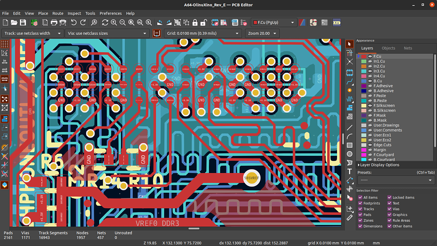
KiCad - Schematic Capture & PCB Design Software
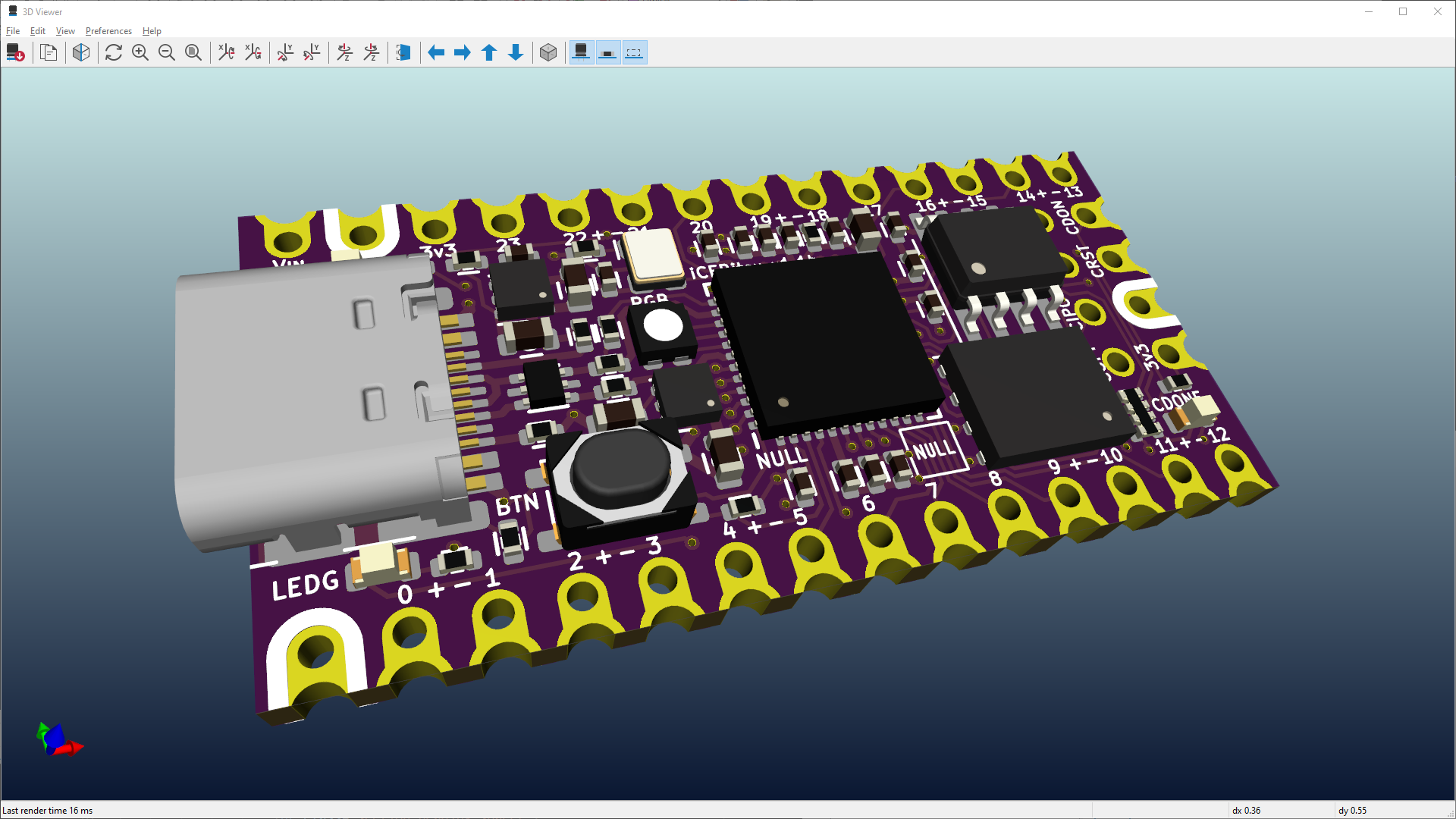 kicad.org
KiCad - Schematic Capture & PCB Design Software
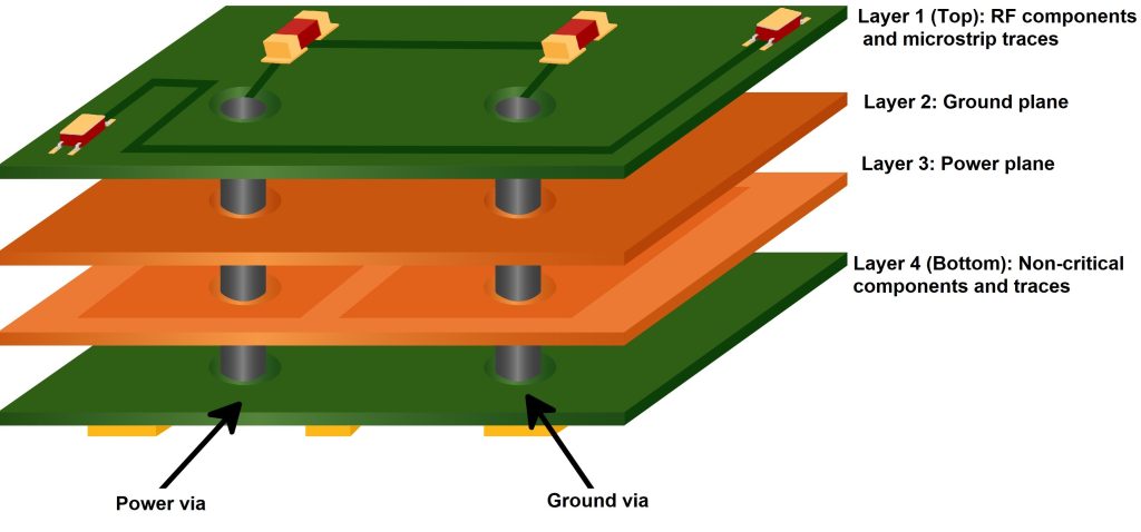
Demystifying PCB Layer Stackup: A Beginner's Guide To Multilayer PCBs
 www.pcbjhy.com
Demystifying PCB Layer Stackup: A Beginner's Guide to Multilayer PCBs ...
How Do I Convert A Schematic To PCB Layout In KiCad (Step By Step) - RayPCB
 www.raypcb.com
How do I convert a Schematic to PCB Layout in KiCad (Step By Step) - RayPCB
Kicad 2 Layer PCB Design: Tips And Best Practices – Hillman Curtis
 hillmancurtis.com
Kicad 2 Layer PCB Design: Tips and Best Practices – Hillman Curtis ...
Etching 555 Astable Timer PCB | EzContents Blog
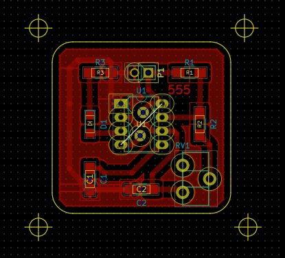 ezcontents.org
Etching 555 astable timer PCB | ezContents blog
10 Automotive PCB Design Guidelines | Sierra Circuits
 www.protoexpress.com
10 Automotive PCB Design Guidelines | Sierra Circuits
KiCad Tutorial - How To Make A 4 Layer PCB In #KiCad - YouTube
 www.youtube.com
KiCad Tutorial - How to make a 4 layer PCB in #KiCad - YouTube
Stencil Alignment Holes In KiCad - PCB Q&A - AISLER Creative Community
 community.aisler.net
Stencil alignment holes in KiCad - PCB Q&A - AISLER Creative Community
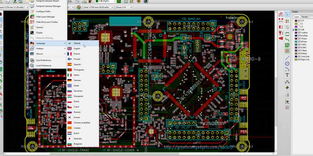
Working With KiCad 7: Importing EAGLE Files - Element14 Community
 community.element14.com
Working with KiCad 7: Importing EAGLE files - element14 Community
Altium Designer Pcb Siliconsafas | Hot Sex Picture
 www.hotzxgirl.com
Altium Designer Pcb Siliconsafas | Hot Sex Picture
Automotive Camera PCB: The Secret Weapon For Smarter Driving
 www.linkedin.com
Automotive Camera PCB: The Secret Weapon for Smarter Driving
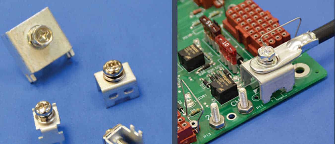
What Is A PCB Screw Terminal:Functions,Types And Install Methods - RayPCB
 www.raypcb.com
What is a PCB Screw Terminal:Functions,Types and Install Methods - RayPCB
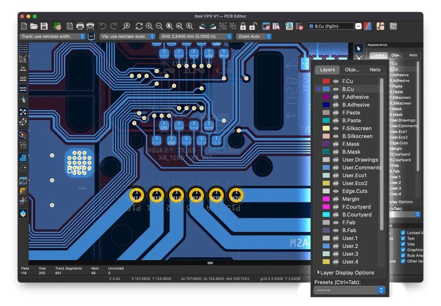
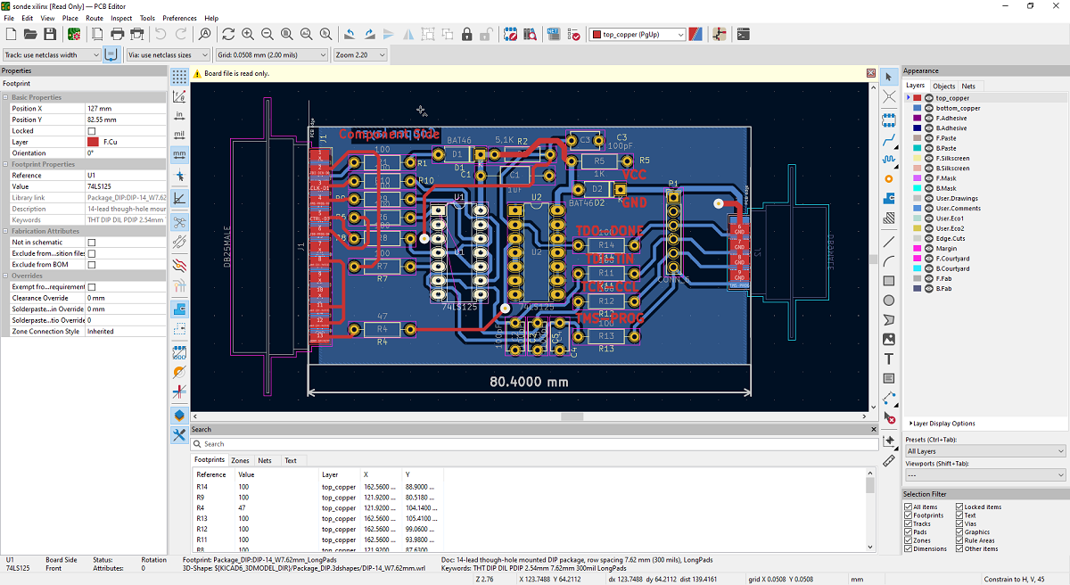
PCB Editor | Master | English | Documentation | KiCad
 docs.kicad.org
PCB Editor | master | English | Documentation | KiCad
EEVblog #1193 - KiCAD PCB 4 Layer Swapping & Stackup - YouTube
 www.youtube.com
EEVblog #1193 - KiCAD PCB 4 Layer Swapping & Stackup - YouTube
Kicad Pcb
 intpik.ru
Kicad pcb
KiCad官方推荐的一些开源的KiCad设计项目
 www.eetree.cn
KiCad官方推荐的一些开源的KiCad设计项目
Pcb Design With Kicad 4-layer Pcb Design In Kicad 5: Quick Thoughts
 pcbways.pages.dev
pcb design with kicad 4-layer pcb design in kicad 5: quick thoughts
Basic KiCad 2-Layer PCB Routing Demonstration - YouTube
 www.youtube.com
Basic KiCad 2-Layer PCB Routing Demonstration - YouTube
4 Layer Pcb Design Tutorial Kicad Pcb Designs | Hot Sex Picture
 www.hotzxgirl.com
4 Layer Pcb Design Tutorial Kicad Pcb Designs | Hot Sex Picture
UX/UI Design News, Articles, Library, Inspiration & Resources
 www.designux.cc
UX/UI Design News, Articles, Library, Inspiration & Resources
PCB Manufacturing Process: A Comprehensive Guide - MKTPCB
 www.mktpcb.com
PCB Manufacturing Process: A Comprehensive Guide - MKTPCB
Beginner’s Guide To PCB Design: 10 Steps To Craft Your Own Printed
 creatiwise.com
Beginner’s Guide to PCB Design: 10 Steps to Craft Your Own Printed ...
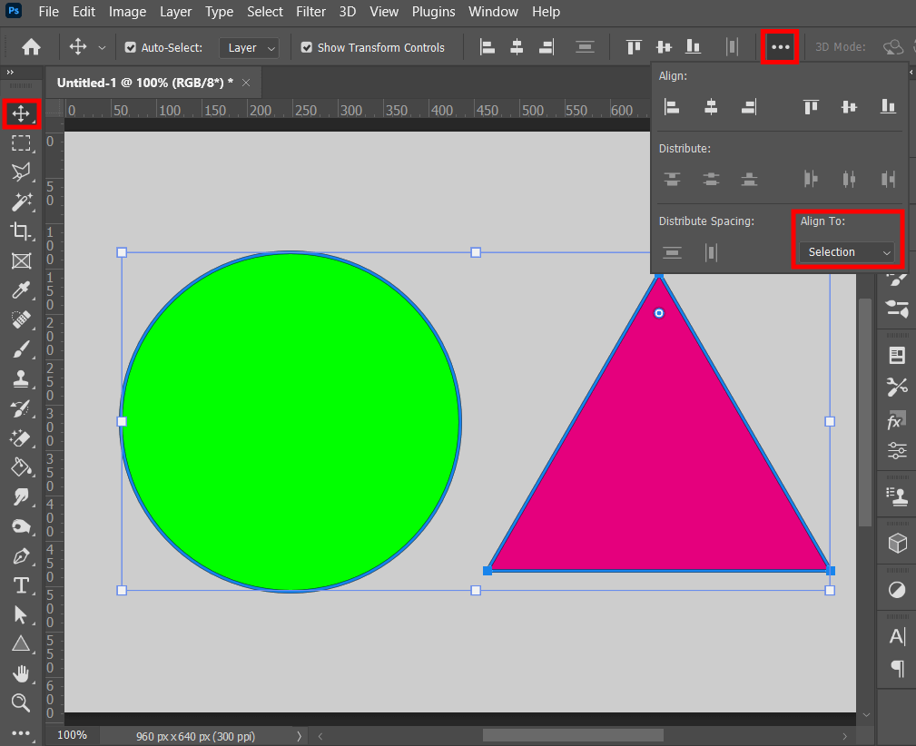
Mastering Layer Alignment In Procreate: A Comprehensive Guide
 www.homeostasislab.com
Mastering Layer Alignment in Procreate: A Comprehensive Guide ...
Kicad 2 Layer PCB Design: Tips And Best Practices – Hillman Curtis
 hillmancurtis.com
Kicad 2 Layer PCB Design: Tips and Best Practices – Hillman Curtis ...
Pcb Design Kicad Tutorial 4 Layer Pcb Design Tutorial Kicad Pcb Designs
 eroppa.com
Pcb Design Kicad Tutorial 4 Layer Pcb Design Tutorial Kicad Pcb Designs ...
pcb manufacturing process: a comprehensive guide. Pcb design with kicad 4-layer pcb design in kicad 5: quick thoughts. Pcb editor